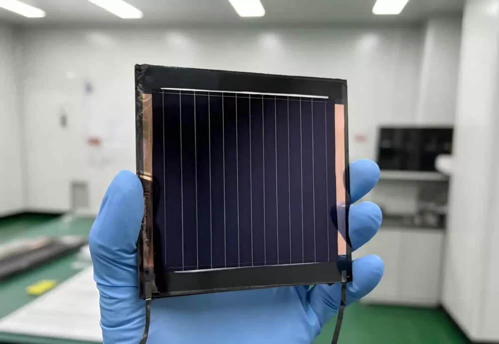
Recently, a team led by Professor Tan Hairen from Nanjing University, in collaboration with Renshuo Photovoltaic (Suzhou) Co., Ltd., achieved a milestone breakthrough in all-perovskite tandem photovoltaic technology. The team successfully fabricated a large-area all-perovskite tandem photovoltaic module measuring 65 square centimeters. Certified by the Japan Electrical Safety & Environment Technology Laboratories (JET), the module demonstrated a steady-state power conversion efficiency of 26.2%, setting a new world record for all-perovskite tandem modules in this size category. The research findings were published online as an "Accelerated Article Preview" in the prestigious international journal *Nature* on June 15, 2026, laying a core process foundation for the industrialization of next-generation, high-efficiency photovoltaic technology.
Large-Area Module Efficiency Enters the 26%+ Tier
As a key pathway for next-generation photovoltaics, all-perovskite tandem solar cells are regarded by the industry as crucial for breaking through the efficiency limits of crystalline silicon, thanks to their broad spectral response, high light-absorption coefficient, and potential for low-cost production. However, prior technological progress was largely confined to small-scale laboratory devices (on the order of square centimeters); scaling up the area introduced challenges—such as poor thin-film uniformity, high interfacial losses, and rapid efficiency degradation—that served as major bottlenecks hindering industrialization.
The 65-square-centimeter all-perovskite tandem module announced here moves beyond the scope of small laboratory samples, approaching the specifications of basic units used in industrial manufacturing. Independent certification by JET, conducted in accordance with IEC standards, confirmed a steady-state power conversion efficiency of 26.2%. This figure is significantly higher than the 20%–22% mass-production efficiency typical of mainstream crystalline silicon modules and substantially surpasses the previous global record for all-perovskite tandem modules of the same size. Data indicates that the module achieved a peak internal laboratory efficiency of 26.6%; the minimal deviation between the certified results and internal laboratory data validates the stability and reproducibility of the technical approach.
Overcoming Industrialization Challenges Through Innovations in Structure and Process
To achieve high efficiency and uniformity in large-area modules, the research team implemented systematic innovations across two key dimensions—device structure and fabrication process—thereby completely redesigning the interfacial connection scheme for all-perovskite tandem modules.
Regarding device structure, the team innovatively adopted a tunneling recombination junction design that eliminates the need for a hole-transport layer. They replaced the ultrathin metal recombination layer found in conventional designs with a functional layer of surface-engineered indium oxide (In₂O₃) nanocrystals and completely removed the PEDOT:PSS hole-transport layer. This structural redesign not only enabled controllable adjustment of the recombination layer's work function—significantly boosting charge extraction efficiency and interfacial transport performance, which raised the module's open-circuit voltage by 42 mV—but also resolved critical industry issues associated with PEDOT:PSS, such as acidic corrosion, high hygroscopicity, and poor long-term stability. Furthermore, it reduced the consumption of precious metals, successfully balancing the goals of high efficiency, long lifespan, and low cost.
In terms of fabrication, the team developed a binary co-solvent system—comprising 2-methoxyethanol and tetrahydrofuran—tailored for lead-tin narrow-bandgap perovskite materials and compatible with industrial blade-coating technology. By precisely regulating the crystallization rate of the perovskite film, this system overcame challenges such as excessively rapid film formation and asynchronous crystallization between layers during large-area production, effectively ensuring the uniform and controllable fabrication of large-sized perovskite films. Test results demonstrated that efficiency fluctuations across a 65-square-centimeter module remained below 5.2%, with film uniformity meeting the fundamental requirements for mass production.
Steadily Transitioning Laboratory Achievements to Mass Production
This breakthrough is the result of deep collaboration between the research team at Nanjing University and industrial partners. Professor Tan Hairen’s team at Nanjing University has long specialized in perovskite tandem technology. Having previously achieved conversion efficiencies exceeding 30% in small-area all-perovskite tandem cells—with results frequently published in top-tier journals like *Nature* and *Science*—the team possesses deep technical expertise. Renshuo Optoelectronics, the entity driving industrialization, has secured hundreds of millions of yuan in Series A funding and established the world’s first R&D and production line for large-area all-perovskite tandem cells, demonstrating engineering capabilities that bridge laboratory processes with mass-production requirements.
This efficiency breakthrough for large-area modules represents more than just an incremental gain in laboratory metrics; it is the result of targeted efforts to address the challenges of large-scale manufacturing. The hole-transport-layer-free structure simplifies the device architecture, while the blade-coating process and binary co-solvent system are directly compatible with mass-production equipment such as roll-to-roll and large-area coating lines. This highly industry-compatible process route clears critical technical hurdles for transitioning all-perovskite tandem modules from the laboratory to gigawatt-scale mass production.
Advancing in Both Terrestrial and Space Photovoltaics
Breakthroughs in all-perovskite tandem technology offer multifaceted value to the photovoltaic industry. For terrestrial applications, higher conversion efficiency translates to a smaller footprint and lower Balance of System (BOS) costs for the same installed capacity, making the technology suitable for diverse scenarios ranging from distributed photovoltaics to utility-scale power plants. Furthermore, the all-perovskite structure eliminates reliance on crystalline silicon substrates, promising reduced raw material costs and lower production energy consumption, thereby driving down the Levelized Cost of Electricity (LCOE).
Beyond terrestrial use, the technology offers significant advantages in space photovoltaics. Perovskite materials possess high light-absorption coefficients, enabling efficient photoelectric conversion with sub-micron thickness; this drastically reduces module weight and simplifies solar array deployment mechanisms, meeting the aerospace sector's critical need for lightweight, high-efficiency photovoltaic systems. The team also plans to further optimize module stability against extreme conditions—such as space radiation, vacuum environments, and thermal cycling—thereby expanding the application scope of this next-generation space photovoltaic technology.
The achievement of this world-record 26.2% efficiency marks my country’s position at the global forefront of large-area all-perovskite tandem photovoltaic module technology. As process optimization and production line adaptation continue to advance, the industrialization of all-perovskite tandem photovoltaic technology is poised to accelerate further, providing a novel technological pathway to support the realization of "dual carbon" goals.


One step to find us,we will respond within 24 hours.
More Contact Details
008613738639386
[email protected]