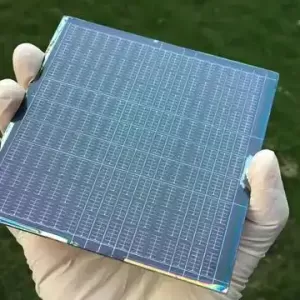
A research team from Nanjing University of Technology has made a breakthrough in the field of perovskite photovoltaic technology. Using a unique "full-vacuum thermal evaporation" technique, the team successfully fabricated a perovskite photovoltaic device with an area of 0.066 square centimeters, achieving a photoelectric conversion efficiency of 25.19%, once again breaking the world record for this technology. This achievement was officially published in the internationally renowned journal *Nature Photonics* on October 21, 2025.

The core of this breakthrough lies in the comprehensive optimization of the "full-vacuum thermal evaporation" technique. According to Guo Qingxun, the corresponding author of the paper and an associate professor at Nanjing University of Technology, this technology is similar to "evaporating" thin films in a vacuum environment: the raw materials are heated, causing them to vaporize in molecular or atomic form and deposited on a substrate to form a uniform and dense thin film structure. Compared with traditional fabrication methods, this technology does not use any solvents throughout the process, allowing for more precise process control and significantly improved film quality. It is considered an ideal path to promote the industrialization of high-performance perovskite photovoltaic devices from the laboratory.
Currently, international laboratories generally employ solution-based methods to fabricate perovskite photovoltaic devices, including spin-coating and coating techniques. Xu Yutian, the first author of the paper and a doctoral student at Nanjing University of Technology, pointed out that solution-based methods typically require the use of toxic solvents such as N,N-dimethylformamide and dimethyl sulfoxide, posing potential risks to health and the environment and limiting their application in large-scale production.
After achieving uniform film formation, further improving photoelectric conversion efficiency became a key challenge for the team. Chen Yonghua, a professor at Nanjing University of Technology and co-corresponding author of the paper, explained that the team innovatively proposed a "reverse layer-by-layer" deposition strategy. He vividly explained, "Traditional methods are like laying 'bricks' before pouring 'cement,' while we do the opposite, depositing 'cement' first and then 'bricks.'" This sequence, combined with self-assembled molecules, effectively promotes the reaction and diffusion between solid raw materials during subsequent annealing, thereby "growing" a high-quality perovskite crystal film.
Notably, the device also exhibits excellent stability. Experimental data shows that after more than 1000 hours of continuous operation, the device retains over 95% of its initial performance, demonstrating excellent long-term operational stability. Furthermore, a 1-square-centimeter device fabricated using the same method achieved an efficiency of 23.38%, showing promising prospects for industrial application.
Huang Wei, co-corresponding author of the paper and academician of the Chinese Academy of Sciences, summarized that this achievement not only broke the world record for all-vacuum thermally evaporated perovskite solar cells but also laid a solid scientific foundation for further optimizing processes, improving device performance, and achieving large-scale manufacturing of large-area, highly efficient, stable, and environmentally friendly perovskite photovoltaic devices. With the continuous maturation of the technology, perovskite photovoltaic technology is expected to inject new impetus into the development of clean energy.


One step to find us,we will respond within 24 hours.
More Contact Details
008613738639386
[email protected]